


B.Tech. Electronics Engineering (VLSI Design and Technology)
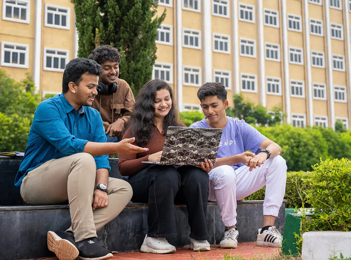
The B.Tech. Electronics Engineering (VLSI Design and Technology) programme at GITAM School of Technology, Visakhapatnam Campus, focuses on developing expertise in circuits, semiconductors, systems, and signal processing. This programme is designed to meet the needs of the rapidly evolving electronics industry, with a curriculum that integrates academic knowledge with practical skills. The curriculum is guided by academic leaders from premier institutions like IITs and NITs and is enhanced through strategic collaborations with industry leaders such as Intel, Capgemini, and Adept Chips.
Eligibility
A minimum of 60% in 10+2 with Physics, Chemistry, and Mathematics subjects and qualification in GAT UG (Engineering) 2024.
Scope of the Programme
The programme offers in-depth knowledge in VLSI design and technology, covering areas such as digital design verification, analog and mixed-signal design, RTL design and synthesis, and electronic design automation. Graduates will be well-prepared to pursue careers in industries related to semiconductor design, electronics manufacturing, and advanced computing systems.
Department Vision
- To excel in Electrical, Electronics and Communication Technologies cultivating innovation with socio-ethical commitment
Department Mission
- M1: Empower the students with knowledge to face real-world challenges for holistic development.
- M2: Conduct multidisciplinary research that makes an impact on society, addressing key challenges through innovative solutions.
- M3: Foster a culture emphasizing empathy, respect, commitment upholding the ethical standards.
Programme Specific Outcomes(PSOs):
At the end of the Programme the students would be able to:
-
PSO1: Demonstrate comprehensive knowledge and practical skills in Electrical and Computer Engineering focusing on the subareas of Electric Vehicle Technology, Industrial Automation and Control and Robotics and apply this knowledge to solve advanced problems.
-
PSO2: Design and translate abstract concepts in electrical machines, power systems, power electronics and computing to real-time circuits & systems and analyze their performance.
-
PSO3: Research and formulate suitable technologies for the implementation of Electrical and Computer Engineering solutions, demonstrating entrepreneurial and research aspects with a commitment to professional ethics and a focus on societal well-being.
Programme Specific Outcomes(PSOs):
At the end of the Programme the students would be able to:
- PSO1: Design and research analog, digital and mixed-signal integrated circuits using different VLSI design methodologies involving industry standard tools balancing tradeoffs in area, power, speed and reliability
- PSO2: Apply research methods to formulate and solve research problems in integrated circuit design of contemporary societal relevance.
- PSO3: Survey and present state of the art circuit/system design procedures for VLSI Design and Fabrication.
Programme Educational Objectives (PEOs)
- PEO 1: To impart comprehensive knowledge of analytical foundations in Electronics Engineering (VLSI Design and Technology) in terms of different VLSI design methodologies in designing efficient and reliable integrated circuits.
- PEO 2: To inculcate critical thinking and problem-solving abilities to handle the real world problems by applying practical skills in different fields of Electronics Engineering (VLSI Design and Technology).
- PEO 3: To impart qualities of teamwork, appreciation of collaboration that entails inter-disciplinary endeavors and the potential impact of technology on society.
- PEO 4: Develop creativity, Research related skills, self- learning, entrepreneurial, leadership skills and values in order to meet the upcoming needs of the country in semiconductor manufacturing.
Key Highlights
Centre of Excellence & Infrastructure
Access to specialized labs such as the VLSI Physical Design Lab, Digital Design and Verification Lab, Analog & Mixed Signal Design Lab, and RTL Design and Synthesis Lab.
Research Centre
Engage in multidisciplinary research with a focus on VLSI design and semiconductor technologies.
Liberal Education Model
Earn 24 credits across different schools, including Business, Humanities, Law, Architecture, and Sciences.
Industry & Academic Collaborations
Collaborations with prestigious organizations like Intel, Capgemini, and the Centre for Development of Advanced Computing.
Venture Development Centre
Participate in a mandatory 02-credit venture development course, encouraging hands-on learning and innovation.
Syllabus
The curriculum includes specialized subjects such as:
- VLSI Physical Design
- Digital Design Verification
- Analog & Mixed Signal Design
- RTL Design & Synthesis
- Electronic Design Automation
- VLSI System Design
Career Options
Graduates from this programme can pursue various career paths, such as:
- VLSI Design Engineer
- Digital Design Verification Engineer
- Analog & Mixed Signal Design Engineer
- RTL Design Engineer
- Semiconductor Process Engineer
- Electronic Design Automation Specialist
Star Recruiters


School Leadership


Multidisciplinary and Interdisciplinary Applied Education


Notable Alumni

Dr . Rajendra Pamula
Professor, Department of CSE

Sri. Mallavarapu Surya Teja
I.A.S

Indrakanti Raghuma
Scientist F
K.Narendra
Vice President
Srinivas Iragavarapu
Sr. SDM, Amazon Code Whisperer
Rajanala Hari Hara Kumar
Software Developer

Eswara N V Geratayya
Director

Sunitha Chirla
Applications Technical Analyst

Rama Krishna Addanki
Senior Solution Architect

Viswa Teju Colluru
CEO and Founder

Kalyan Nallaparaju
Associate Director

Eswar Sunil Kumar
VP & Head of India Operations

Prashant Ganji
Senior Scientist - Downstream Process Development

Aravind kshatri
Senior Scientist

Dr. Sushmitha Sundar
Head (Life Sciences) RICH,

Rajesh Chitta
Senior Technology Manager

T.Srinivasan
Registrar

Dr K D D Srikanth
Adjunct faculty

Lakshmi Prasad
Deputy Manager

Nirmal Kumar
Manager

Gangadhar
Deputy Manager

Dr. Manideep Tummalapudi
Assistant Professor , Construction Management

M.Praveen Kumar
IES

KNV Siva Kumar
Assistant Vice President
Dhiraj Varma
Entrepreneur, Director - Technical & Operations
Niranjan Reddy Renati
Grad Year: 2002, Vice President / Country Head at Olam Group, Thailand
Sindhura Polasana Palli
Grad Year: 2002, Sr. Director - Marketing - Keurig Dr Pepper
Maurya Chandra Pydah
Grad Year: 2004, Associate Director at Greenko Group

Krishna Devareyalu Lavu
Grad Year: 2004, MP - TDP, Andhra Pradesh, India
Adarsh Atluri
Grad Year: 2006, Director - Harmony Ventures, Gurgaon, Haryana, India
Srinivasa Raju Namburi
Grad Year: 2006, CEO & Co-founder - BridgeThings Hyderabad, India
Amaranath Dabbara
Grad Year: 1990, Group Software Engineering Manager - Qualtrics, Seattle , USA Greater Seattle Area

Bharath Satti
Grad Year: 1999, Chief Architect, Director R&D - Plymouth Rock Assurance, Greater Boston

Narasimha Bhogavalli
Grad Year: 1990, Director - Tekdynamics Inc, Irving, United States

Vaibhav Sisinty
Grad Year: 2015, CEO - Growth School, Bengaluru, India
Mr. G Srinivasa Rao,
Vice President

Mr. B Raghu Kiran
IRS

Prof. G Sasibhushana
Professor

Mr. D Ashok
Senior Physical Design Engineer

Mr. Murali P
VP Engineering - VLSI

Ms. B V Srilekha
Analog Design Engineer
Dr. Edwin Vijay Kumar
AGM
Dr K V Srinivas
Scientist C

Narasimha Eswara Sarma Munukutla
SCADA Specialist/Principal Engineer

Dr K Narendra Swaroop
Senior Program Manager- Quality

A. Venkata Ramana
Director - Embedded Software
Vasupalli Ganesh Kumar
EX. MLA, VIZAG SOUTH

TLN Sharma
Designation: Software Group Manager Current Organisation: Schaeffler AG, USA
Vijay Rudra Raju
Associate Director Ericcson
B.SREENIVASA REDDY
Scientist H ADA-DRDO, Bengaluru

B.Raghu Kiran
IRS, Joint Commissioner, GST-Hyderabad
Shekhar Movva
Founder and CEO

Dr. Vidya kumari
Associate Professor

Mr. Anand Stanley
President

Smt. V. Shanti
Scientist-F

Prof. P.V.G.D. Prasad Reddy
Former Vice Chancellor
Mr. Partha Datta
Head, Engineering, Design
Infrastructure and Facilities


Fee Structure
B.Tech. Electronics and Engineering (VLSI Design and Technology)
1st Year
₹2,83,500
2nd Year
₹2,97,600
3rd Year
₹3,12,400
4th Year
₹3,28,000
Scholarships
Merit-Based Scholarships
The scholarship from GAT/National/State Entrance Tests applies only in the first year. To continue receiving it in subsequent years, a minimum CGPA of 8.0 must be maintained.
Apart from the above, the following scholarships are also offered to eligible students.
- Employee Children Scholarships: (60%, 40%, and 20%)
- Loyalty Scholarships: (10% for Any alumni returning to do higher studies/Children of Alumni/Real siblings (Not applicable to step siblings or cousins)/Children of retired employees of GITAM/Spouse of GITAM employees).
- Sports Scholarships: (100%, 75%, 50%, 25% and 15%)
Need-Based Scholarships
- To be eligible for the need-based scholarship, the combined income of both parents/guardians of the eligible student/If the student is married, the combined income of the family, i.e., the student's and spouse's income, must be less than 8.00 LPA.
- The candidates admitted through merit scholarship in the slabs of 75%, 60%, 40%, 25%,and 15%, and the parents/guardians combined income is less than the prescribed limits are eligible for the additional need-based scholarship.
| Scholarship % | Upgraded Scholarship % |
|---|---|
| 75% | 100% |
| 60% | 75% |
| 40% | 60% |
| 25% | 40% |
| 15% | 25% |
Scholarships For Accommodation
- In addition, students awarded need-based scholarships after merit scholarships will receive an additional 20% scholarship specifically allocated for hostel fees at GITAM for slabs: 15%, 25%, 40%, and 60%.
- Students awarded 75% & 100% scholarships are also awarded the same percentage in the hostel and food charges.
| Year | Scholarship % | GAT 2025 Score | JEE(Main) 2025 | AP / TS EAPCET | SAT 2025 | NID DAT 2025 |
|---|---|---|---|---|---|---|
| 2025-26 | 100 | 141 - 200 | >=97.00 | 1 – 100 | 1501-1600 | >=97 |
| 75 | 131 - 140 | 94-96.99 | 101 - 250 | 1451 - 1500 | 94 - 96 | |
| 60 | 121 - 130 | 92 - 93.99 | 251 - 1000 | 1401 - 1450 | 92 - 93 | |
| 40 | 111 - 120 | 90 - 91.99 | 1001 - 2500 | 1351 - 1400 | 90 - 91 | |
| 25 | 101 - 110 | 88 - 89.99 | 2501 - 5000 | 1301 - 1350 | 87 - 89 | |
| 15 | 86 - 100 | 85 - 87.99 | 5001 - 25000 | 1200 - 1300 | 84 - 86 |
Note: Terms & Conditions Applied
Lateral Entry
| Year | Scholarship % | GAT 2025 Score | AP/TS ECET & DCET 2025 Branch Rank | State Technical Board % Except (AP,TS & KA) |
|---|---|---|---|---|
| 2025-26 | 100 | 141 - 200 | 1 – 100 | 95 - 100 |
| 75 | 131 - 140 | 101 - 500 | 91 - 94.99 | |
| 60 | 121 - 130 | 501 - 1000 | 88 - 90.99 | |
| 40 | 111 - 120 | 1001 - 1500 | 83- 87.99 | |
| 25 | 101 - 110 | 1501 - 3000 | 80 - 82.99 | |
| 15 | 86 - 100 | 3001 - 5000 | 70 - 79.99 |
Note: Terms & Conditions Applied
